Technology Summary
Electronic devices are getting smaller and more energy-efficient. This means they are more susceptible to single-event upsets- a malfunction caused by ionizing particles in the atmosphere interfering with electronic systems. The need increases as these devices get smaller, since particles that cause these upsets can even come from the packages that house the devices themselves. This is especially prevalent in the aerospace industry, since working at higher altitudes means increased exposure to cosmic ray particles.
The Invention
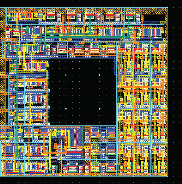
SEUSS is a latch that can be configured in a number of ways familiar to electronic engineers, a latch that suppresses these single-event upsets. The beauty of SEUSS is that it gives electrical engineers a unique freedom of design, since it can behave like any known latch. It offers single-event upset tolerance while maintaining flexibility in design, and saves money in the process. Single Event Upset Suppression System (SEUSS) cells are designed to be immune to Single Event Upsets (SEU). CMOS transistors are configured to operate as a SEU-tolerant SR latch. The SEUSS cells come in two different variations. One type of SEUSS cell emulates a cross-coupled NOR gate SR flip-flop (SEUSSNor). The other type emulates a cross-coupled NAND gate SR flip-flop (SEUSSNand). This flexible device, when configured as an SEU tolerant SR latch, can be converted into any known type of latch.
Benefit
- Can behave like any known latch (SR latch, D latch, T flip flop, etc.)
- Previously, designing a custom radiation-tolerant system could cost billions of dollars
Applications and Industries
- Electronic devices
- Electrical Engineering
- Aerospace Industry
Category: Engineering Technologies, Detector Technologies
Tags and keywords: Logic Gate, Asynchronous, Latch, Flip-flop, Single Event Upset, SEU, Design Tolerance, Single Event Effects, Digital Circuit
Invention Details
Patent Status: Patented
Contact:
Aaron G Sauers, CLP
630-840-4432
asauers@fnal.gov
Fermilab, MS 312 – PO Box 500
Batavia, IL 60510